
Extreme ultraviolet lithography (EUVL, also known simply as EUV) is a technology used in the semiconductor industry for manufacturing integrated circuits (ICs). It is a type of photolithography that uses 13.5 nm extreme ultraviolet (EUV) light from a laser-pulsed tin (Sn) plasma to create intricate patterns on semiconductor substrates. ASML, Intel, TSMC, and Samsung have all poured money into EUV technology being the key players in the market. Significant large-scale investments in semiconductor R&D, the EUV adoption is continuing to gain momentum and will provide the basis for future breakthroughs in semiconductor technology.
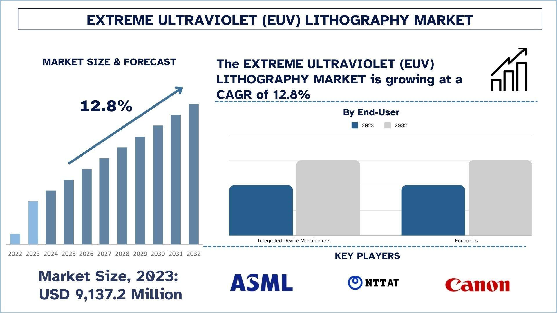
According to the UnivDatos, rising demand for advanced semiconductor nodes, significant investments in R&D and manufacturing, and the rapid adoption of AI, 5G, and IoT technologies would drive the global scenario of the Extreme Ultraviolet Lithography market. As per their “Extreme Ultraviolet Lithography Market” report, the global market was valued at USD 9,137.2 Million in 2023, growing at a CAGR of 12.8% during the forecast period from 2024 - 2032 to reach USD Million by 2032.
For More Detailed Analysis in PDF Format, Visit- https://univdatos.com/reports/Extreme-Ultraviolet-EUV-Lithography-Market?popup=report-enquiry
Government Policies fostering the growth of the Extreme Ultraviolet Lithography market
Funding and incentives provided by government policies, as well as strategic support for the semiconductor industry, are very important for the growth of the Extreme Ultraviolet (EUV) lithography market. Key initiatives include:
1. CHIPS Act (United States)
There is a major U.S. policy on the table to support domestic semiconductor manufacturing—created by Cong. Senator Todd Young of Indiana developed over the past five years, the CHIPS Act (Creating Helpful Incentives to Produce Semiconductors for America Act). It also offers a sizeable bundle of financial incentives, such as grants and tax credits, to semi companies to invest in building advanced fabrication plants and push the envelope on advanced technology fronts like EUV lithography. The policy is meant to reduce the U.S.'s reliance on foreign semiconductor manufacturing and help the country boost its standing in global high-tech manufacturing.
2. Made in China 2025 (China)
As part of China’s “Made in China 2025” initiative, China aims to substantially raise its technological level and diminish its reliance on foreign semiconductor technology. In this regard, China has been investing heavily in semiconductor manufacturing including adopting EUV technology. Buy a cut-and-dried story in the state government's fondness for domestic companies, which includes EUV adoption for advanced chip production and which they support with funding and favorable policies to drive the semiconductor industry.
3. Semiconductor Industry Policies in South Korea and Japan
Similarly, semiconductor development and manufacturing are being prioritized by South Korea and Japan. Samsung and South Korean rival SK Hynix are also big players in the US, both from the government subsidies and investments there intended to bolster domestic semiconductor production. The government in Japan is supporting the adoption of EUV technology by funding its research and development along with the funding necessary for infrastructure to improve the capabilities of semiconductor manufacturers to continue to be globally competitive.
4. European Union Initiatives
Also, the European Union has understood the importance of semiconductor technology and has launched the Digital Compass Plan and Horizon Europe programs. They will fund increased semiconductor R&D investments like EUV lithography, to support the strengthening of the EU’s semiconductor manufacturing ecosystem. The European Commission is striving to advance the development of highly sophisticated semiconductor technologies, to maintain European leadership in the field through significant investments.
All of these government policies work to support this kind of environment that enables EUV technology adoption and enables the semiconductor industry to continue to innovate to meet the ever-increasing demand for smaller, more powerful chips.
Explore the Comprehensive Research Overview - https://univdatos.com/reports/Extreme-Ultraviolet-EUV-Lithography-Market
Related Reports:
India Semiconductor Market: Current Analysis and Forecast (2024-2032)
Chemical Mechanical Planarization (CMP) Slurry Market: Current Analysis and Forecast (2024-2032)
Microelectronics Market: Current Analysis and Forecast (2024-2032)
Conclusion
The article concludes that government policies are critical to the development of the Extreme Ultraviolet (EUV) lithography market growth by providing strategic support and financial incentives to encourage domestic semiconductor manufacturing. Investments in cutting-edge technologies like EUV are being spurred by initiatives like the CHIPS Act in the U.S., China’s Made in China 2025, and semiconductor-focused policies in South Korea, Japan, and the EU. In addition to sustaining competitiveness in global microchip markets, these policies encourage innovation in microchip manufacturing. Consequently, EUV lithography technology will assume a key role in defining the evolution of advanced semiconductor production and meeting the requirements of upcoming technologies.
Contact Us:
UnivDatos
Contact Number - +19787330253
Email - [email protected]
Website - www.univdatos.com